- 您现在的位置:买卖IC网 > Sheet目录1213 > EVAL-ADE7751ZEB (Analog Devices Inc)BOARD EVALUATION FOR ADE7751
�� �
�
�ADE7751�
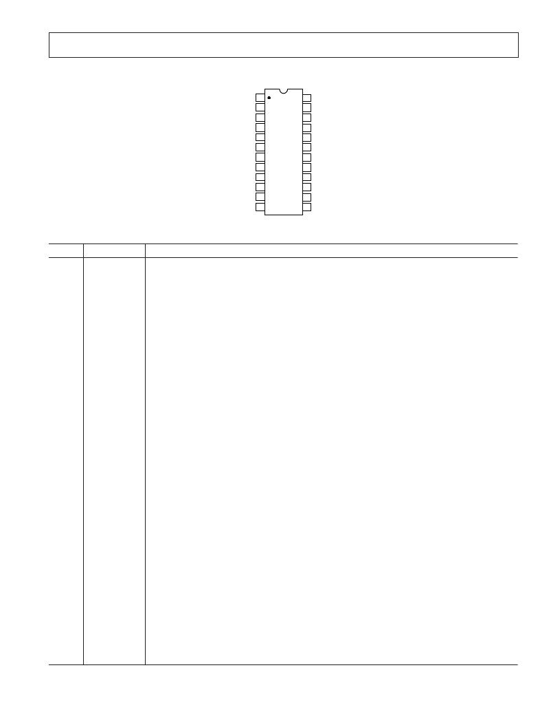
�PIN� CONFIGURATION�
�DV� DD�
�1�
�24�
�F1�
�AC/� DC� 2�
�23�
�F2�
�AV� DD�
�3�
�22�
�CF�
�V1A� 4�
�21�
�DGND�
�V1B� 5�
�ADE7751�
�20�
�REVP�
�V1N� 6�
�TOP� VIEW�
�19� FAULT�
�V2N� 7� (Not� to� Scale)� 18� CLKOUT�
�V2P� 8�
�RESET� 9�
�REF� IN/OUT� 10�
�AGND� 11�
�SCF� 12�
�17�
�16�
�15�
�14�
�13�
�CLKIN�
�G0�
�G1�
�S0�
�S1�
�PIN� FUNCTION� DESCRIPTIONS�
�Pin� No.�
�1�
�2�
�3�
�4,� 5�
�6�
�7,� 8�
�9�
�10�
�11�
�12�
�REV.� 0�
�Mnemonic�
�DV� DD�
�AC/� DC�
�AV� DD�
�V1A,� V1B�
�V1N�
�V2N,� V2P�
�RESET�
�REF� IN/OUT�
�AGND�
�SCF�
�Description�
�Digital� Power� Supply.� This� pin� provides� the� supply� voltage� for� the� digital� circuitry� in� the� ADE7751.�
�The� supply� voltage� should� be� maintained� at� 5� V� ±� 5%� for� specified� operation.� This� pin� should� be�
�decoupled� with� a� 10� μ� F� capacitor� in� parallel� with� a� ceramic� 100� nF� capacitor.�
�High-Pass� Filter� Select.� This� logic� input� is� used� to� enable� the� HPF� in� Channel� 1� (the� current�
�channel).� A� Logic� 1� on� this� pin� enables� the� HPF.� The� associated� phase� response� of� this� filter� has�
�been� internally� compensated� over� a� frequency� range� of� 45� Hz� to� 1� kHz.� The� HPF� filter� should� be�
�enabled� in� energy� metering� applications.�
�Analog� Power� Supply.� This� pin� provides� the� supply� voltage� for� the� analog� circuitry� in� the� ADE7751.�
�The� supply� should� be� maintained� at� 5� V� ±� 5%� for� specified� operation.� Every� effort� should� be� made�
�to� minimize� power� supply� ripple� and� noise� at� this� pin� by� the� use� of� proper� decoupling.� This� pin�
�should� be� decoupled� to� AGND� with� a� 10� μ� F� capacitor� in� parallel� with� a� ceramic� 100� nF� capacitor.�
�Analog� Inputs� for� Channel� 1� (Current� Channel).� These� inputs� are� fully� differential� voltage� inputs�
�with� a� maximum� signal� level� of� ±� 660� mV� with� respect� to� pin� V1N� for� specified� operation.� The�
�maximum� signal� level� at� these� pins� is� ±� 1� V� with� respect� to� AGND.� Both� inputs� have� internal� ESD�
�protection� circuitry� and� an� overvoltage� of� ±� 6� V� can� also� be� sustained� on� these� inputs� without� risk� of�
�permanent� damage.�
�Negative� Input� Pin� for� Differential� Voltage� Inputs� V1A� and� V1B.� The� maximum� signal� level� at� this�
�pin� is� ±� 1� V� with� respect� to� AGND.� The� input� has� internal� ESD� protection� circuitry� and� an� overvoltage�
�of� ±� 6� V� can� also� be� sustained� without� risk� of� permanent� damage.� This� input� should� be� directly� con-�
�nected� to� the� burden� resistor� and� held� at� a� fixed� potential,� i.e.,� AGND.� See� Analog� Input� section.�
�Negative� and� Positive� Inputs� for� Channel� 2� (Voltage� Channel).� These� inputs� provide� a� fully� differ-�
�ential� input� pair.� The� maximum� differential� input� voltage� is� ±� 660� mV� for� specified� operation.� The�
�maximum� signal� level� at� these� pins� is� ±� 1� V� with� respect� to� AGND.� Both� inputs� have� internal� ESD�
�protection� circuitry� and� an� overvoltage� of� ±� 6� V� can� also� be� sustained� on� these� inputs� without� risk� of�
�permanent� damage.�
�Reset� Pin� for� the� ADE7751.� A� logic� low� on� this� pin� will� hold� the� ADCs� and� digital� circuitry� in� a�
�reset� condition.� Bringing� this� pin� logic� low� will� clear� the� ADE7751� internal� registers.�
�Provides� Access� to� the� On-Chip� Voltage� Reference.� The� on-chip� reference� has� a� nominal� value� of�
�2.5� V� ±� 8%� and� a� typical� temperature� coefficient� of� 30� ppm/� °� C.� An� external� reference� source� may� also�
�be� connected� at� this� pin.� In� either� case,� this� pin� should� be� decoupled� to� AGND� with� a� 1� μ� F� ceramic�
�capacitor� and� 100� nF� ceramic� capacitor.�
�Provides� the� Ground� Reference� for� the� Analog� Circuitry� in� the� ADE7751,� i.e.,� ADCs� and� Refer-�
�ence.� This� pin� should� be� tied� to� the� analog� ground� plane� of� the� PCB.� The� analog� ground� plane� is�
�the� ground� reference� for� all� analog� circuitry,� e.g.,� antialiasing� filters,� current� and� voltage� trans-�
�ducers,� and� more.� For� good� noise� suppression,� the� analog� ground� plane� should� only� be� connected� to�
�the� digital� ground� plane� at� one� point.� A� star� ground� configuration� will� help� to� keep� noisy� digital�
�return� currents� away� from� the� analog� circuits.�
�Select� Calibration� Frequency.� This� logic� input� is� used� to� select� the� frequency� on� the� calibration�
�output� CF.� Table� IV� shows� how� the� calibration� frequencies� are� selected.�
�–5� –�
�发布紧急采购,3分钟左右您将得到回复。
相关PDF资料
EVAL-ADE7752AEBZ
BOARD EVALUATION FOR ADE7752A
EVAL-ADE7753ZEB
BOARD EVALUATION AD7753
EVAL-ADE7754EBZ
BOARD EVALAUTION FOR ADE7754
EVAL-ADE7755ZEB
BOARD EVALUATION FOR AD7755
EVAL-ADE7758ZEB
BOARD EVAL FOR AD7758
EVAL-ADE7759EBZ
BOARD EVALUATION FOR ADE7759
EVAL-ADE7762EBZ
BOARD EVALUATION FOR ADE7762
EVAL-ADE7763ZEB
BOARD EVALUATION FOR ADE7763
相关代理商/技术参数
EVAL-ADE7752AEB
制造商:Analog Devices 功能描述:EVAL BD THREE PHASE ACTIVE ENERGY MET IC - Bulk
EVAL-ADE7752AEBZ
功能描述:BOARD EVALUATION FOR ADE7752A RoHS:是 类别:编程器,开发系统 >> 评估演示板和套件 系列:- 标准包装:1 系列:- 主要目的:电信,线路接口单元(LIU) 嵌入式:- 已用 IC / 零件:IDT82V2081 主要属性:T1/J1/E1 LIU 次要属性:- 已供物品:板,电源,线缆,CD 其它名称:82EBV2081
EVAL-ADE7752EB
制造商:AD 制造商全称:Analog Devices 功能描述:Three Phase Energy Metering IC with Pulse Output
EVAL-ADE7753ZEB
功能描述:BOARD EVALUATION AD7753 RoHS:是 类别:编程器,开发系统 >> 评估演示板和套件 系列:- 标准包装:1 系列:- 主要目的:电信,线路接口单元(LIU) 嵌入式:- 已用 IC / 零件:IDT82V2081 主要属性:T1/J1/E1 LIU 次要属性:- 已供物品:板,电源,线缆,CD 其它名称:82EBV2081
EVAL-ADE7754EB
制造商:Analog Devices 功能描述:EVALUATION BOARD FOR POWER METERING, POLYPHASE MULTIFUNCTION ENERGY METERING IC WITH SERIAL PORT 制造商:Analog Devices 功能描述:PWR METERING, POLYPHASE MULTIFUNCTION ENERGY METERING IC W/ - Bulk
EVAL-ADE7754EBZ
功能描述:BOARD EVALAUTION FOR ADE7754 RoHS:是 类别:编程器,开发系统 >> 评估演示板和套件 系列:- 标准包装:1 系列:- 主要目的:电信,线路接口单元(LIU) 嵌入式:- 已用 IC / 零件:IDT82V2081 主要属性:T1/J1/E1 LIU 次要属性:- 已供物品:板,电源,线缆,CD 其它名称:82EBV2081
EVAL-ADE7755EB
制造商:Analog Devices 功能描述:EVAL BOARD ENERGY METERINGW/PULSE OUTPUT - Bulk
EVAL-ADE7755EBZ
制造商:AD 制造商全称:Analog Devices 功能描述:Energy Metering IC with Pulse Output